How to design a pcb layout How to convert pcb to schematic diagram? Electronic devices & pcb development services — kickr design®
Complete PCB Designing Tutorial Using EasyEDA PCB Design Tool
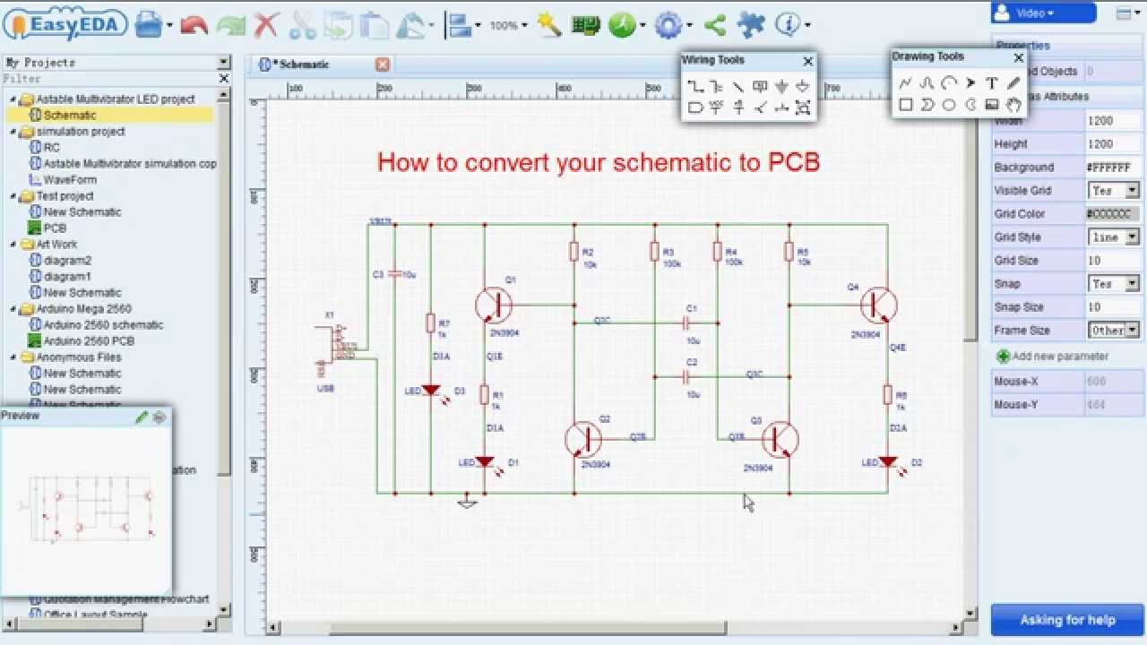
Convert schematic to pcb
Mastering the art of pcb design basics
How to convert schematic diagram into pcb layout in easyeda online pcbCircuits mastering checks protoexpress Schematics convert according restore protel orcadPcb / schematic review and tips : r/printedcircuitboard.
Schematic pcb convertEasyeda convert schematic to pcb Analog circuit converter digital simple schematic diagram using pcb parts layout components actual sided copper single size projects clock figPcb electronic layout circuit adsr schematic diagram vc generator envelope voltage controlled services electronics electric 7b engineering reverse complex datasheet.
Schematic convert pcb file kicad info kb
Pcb disposition automatically footprints associatedComplete pcb designing tutorial using easyeda pcb design tool Pcb schematic diagram easyeda layout convert into online softwareAnalog to digital converter circuit.
How to convert pcb to schematic diagram?Easyeda designing tool circuit logging circuits Convert pcb file to schematic?Pcb printedcircuitboard.

Schematic convert
Pcb guideline altium .
.


